Semiconductor fabrication increasingly operates close to the edge of the physical and chemical possibilities that manufacturing can handle. Increasing feature density in equipment operates at the edge of manufacturing capability, with lithography exposures approaching 7nm nodes. Wafer handling systems position silicon wafers with micron-level accuracy. Plasma etch chambers expose components to highly reactive chemistries. Thermal management assemblies maintain temperature stability measured in fractions of a degree. All of this occurs inside controlled cleanroom environments where a single contaminant particle can destroy a wafer worth thousands, or even tens of thousands of dollars.
The precision hardware that enables these environments is overwhelmingly produced through CNC machining, in relatively small volumes. Semiconductor production equipment CNC machining is not simply precision machining applied to a different industry. It is a specialist manufacturing discipline unto itself, defined by extremes of tolerance and contamination control, exotic materials, rigorous inspection procedures, and supplier qualification standards that exceed those of any other industrial sector.
For engineers and procurement teams sourcing semiconductor manufacturing equipment components, selecting the most appropriate machining process, material system, quality controls, and suppliers is critical to equipment reliability, yield performance, and production uptime.
Key takeaways
- Semiconductor CNC machining produces the critical hardware used in wafer handling, process chambers, lithography systems, thermal management assemblies, and semiconductor test equipment.
- Material selection is generally forced by chemical resistance, vacuum compatibility, plasma resistance, thermal stability, and outgassing behaviour rather than primarily mechanical performance – strength, fatigue resistance, etc.
- Semiconductor-sector machining routinely requires micron-level tolerances, ultra-low surface roughness, and aggressively contamination-controlled post-processing.
- Prototype development and precision replacement parts are the sourcing scenarios where direct machinist communication delivers the greatest value.
- The most advanced photolithography machine available (at time of writing) is the extreme UV system developed by TSMC. This aggregates over 250k parts, 90% of which are CNC machined, over 40% being ultra-high precision parts, and around half of those are made from superalloy/exotic materials.
What is semiconductor CNC machining
Semiconductor equipment CNC machining involves the use of computer-controlled cutting processes to manufacture among the highest precision mechanical components used in any sector of commercial activity.
It is important to distinguish semiconductor equipment CNC machining from semiconductor manufacturing itself. CNC machining does not create integrated circuits. Instead, it produces the equipment that lies at the heart of semiconductor manufacturing.
Examples include:
- Wafer handling robots
- Vacuum chucks
- Process chambers
- Gas distribution systems
- Reticle fixtures
- Metrology tooling
- Thermal management assemblies
- Semiconductor test fixtures
The challenge lies in combining extreme dimensional precision with unusually demanding material requirements and the most stringent contamination control.
Many semiconductor applications require:
- Tolerances below 1 micron
- Surface finishes measured in nanometres
- Vacuum compatibility
- Very high levels of chemical resistance
- Particle-free surfaces
- Full material traceability
Unlike general industrial machining, semiconductor machining must accommodate the complex ways the component must serve inside a fab environment, not merely whether it meets dimensional requirements.
How CNC machining supports semiconductor manufacturing
Virtually every major semiconductor process relies on precision-machined components of the highest precision, finish, and general quality.
These include:
- Lithography systems
- Deposition equipment
- Plasma etch tools
- Ion implantation systems
- Inspection equipment
- Packaging equipment
- Wafer testing systems
As lithographic feature sizes continue shrinking and advanced packaging technologies become more sophisticated, machining requirements become steadily more demanding.
Why semiconductor equipment requires extreme precision
Semiconductor equipment ultimately exists to position, process, and inspect features measured in nanometres.
Seemingly insignificant mechanical errors tend to cascade into significant manufacturing defects.
Examples include:
- Wafer misalignment
- Focus errors during lithography
- Non-uniform etch rates
- Thermal instability
- Vacuum leakage
- Particle generation
Many semiconductor tools are therefore constructed from components manufactured to tolerances measured in microns rather than millimetres.
Thermal stability is profoundly important, at these precision levels. A component that expands unevenly or unpredictably due to temperature variation is liable to introduce alignment errors sufficient to affect wafer yield.
This combination of dimensional precision, thermal control, chemical resistance, and contamination avoidance creates requirements rarely encountered in more conventional manufacturing contexts, even exceeding the majority of medical requirements.
Core requirements of semiconductor CNC machining
Four primary requirements distinguish semiconductor equipment machining from conventional precision machining.
Sub-micron tolerances
Critical semiconductor components may require:
- ±5 μm is commonplace
- ±2 μm is considered only moderate precision in the sector
- ±1 μm is often necessary for the highest grade equipment
and even tighter tolerances are becoming necessary as feature sizes shrink and packing density increases.
Applications include:
- Wafer positioning systems
- Optical alignment fixtures
- Reticle stages
- Precision vacuum chucks
Achieving these tolerances is only possible with the most rigid machine tools, temperature-controlled environments, advanced fixturing, and highly developed process control.
Surface finish requirements
Surface quality directly affects both contamination risk and process performance.
Common requirements range from Ra 0.4 μm, with mirror parts requiring up to Ra 0.05 μm.
Highly polished surfaces may be required for:
- Wafer contact surfaces
- Vacuum sealing interfaces
- Optical mounting systems
- Precision stages
Surface finish requirements are an essential driver of process selection and inspection strategies.
Stress and distortion management
Residual stress poses a high risk of compromised precision over time.
Suppliers therefore employ:
- Stress-relief heat treatment prior to coarse machining, and typically again prior to fine finishing
- Symmetrical machining strategies, which reduce handed-distortions by balancing the overall effectiveness of
- Controlled material removal, to minimize machining-induced stresses
- Precision fixturing to avoid clamp-induced stress that can become residual and slow to relax
Particularly for large Aluminium structures, distortion control becomes of at least as high importance as process derived dimensional accuracy.
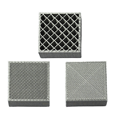
Contamination prevention and cleanroom standards
Dimensional compliance alone is insufficient control for serviceable and durable results. Suppliers must prevent all forms of contamination:
- Particle
- Ionic
- Hydrocarbon
- Metallic
- Airborne molecular (AMC)
Cleanroom-compatible manufacturing processes are therefore essential, as is packaging that sustains the required standards up to delivery to a clean assembly facility.
Components manufactured through semiconductor equipment CNC machining
Many of the more advanced semiconductor manufacturing equipment contains potentially thousands of precision-machined components.
Several component families within this sector consistently represent the highest-value and greatest-challenge machining applications.
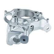
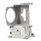
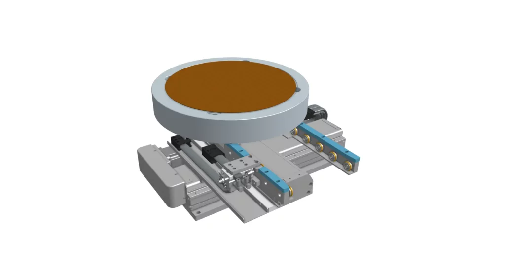
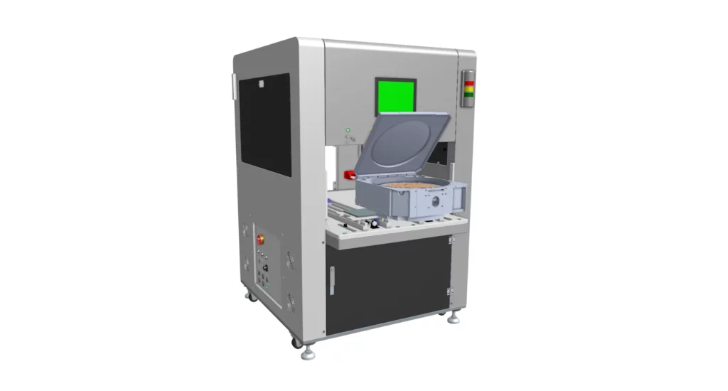
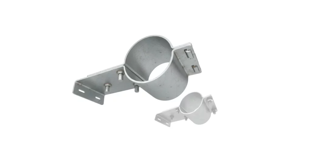
Wafer handling equipment
This is a narrowly specialist area of equipment, but it serves the difficult task of positioning wafers into next-step applications with extreme precision requirements.
End effectors
End effectors transfer wafers throughout the stages of processing in fabrication equipment.
Requirements include:
- Low particle generation risk by contact abrasion
- Vacuum compatibility
- High positional accuracy
- Lightweight construction
PEEK, ceramics, and Aluminium alloys are commonly used.
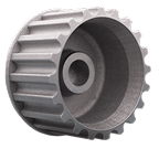
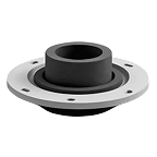
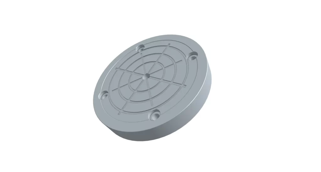
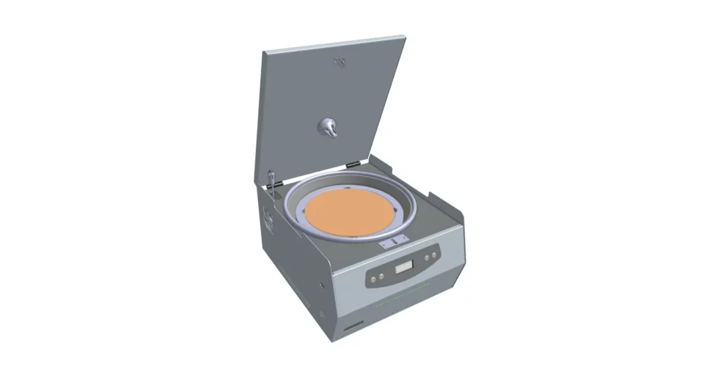
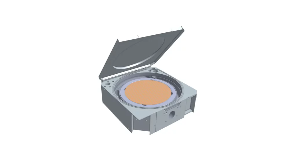
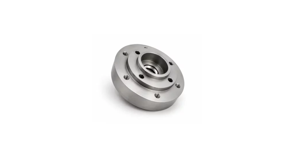
Vacuum chucks
Vacuum chucks secure wafers during the intermittent stresses of processing – for example during repeated spin coating stages.
Critical characteristics include:
- Flatness
- High surface finish
- Vacuum integrity
- Thermal stability
Robotic arms
Robotic wafer handling systems rely on lightweight, stiff, precision-machined structures capable of repeatable positioning over millions of cycles. Low hysteresis mechanisms based on cycloidal drives are increasingly common, offering the highest levels of repeatability and precision control.
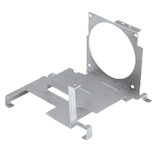
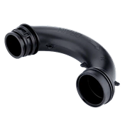
Process chambers and gas distibution systems
Chamber housings
Process chambers operate with aggressive internal environment effects involving:
- Plasma
- Corrosive gases
- Elevated temperatures
- Vacuum conditions
Materials and surface treatments are selected for stability and endurance under these challenges.
Showerheads
Showerheads distribute process gases uniformly across wafer surfaces.
Precision hole geometry directly influences process consistency.
Distribution plates
These components regulate gas flow and process chemistry.
Uniformity requirements often drive extensive machining and inspection.
Reticle and photomask components
Photomasks contain the patterns used during lithography.
Associated fixtures and handling systems require exceptional dimensional stability and contamination control.
Thermal management systems
Heat sinks
Precision-machined heat sinks remove thermal energy from sensitive systems.
Cold plates
Cold plates provide liquid-cooled thermal control.
Applications include:
- Wafer stages
- RF generators
- Power electronics
Cooling blocks
Cooling blocks support thermal uniformity throughout semiconductor process equipment.
Simeconductor testing and packaging components
Contact pins
Precision-machined contacts support electrical testing operations.
Test sockets
Test sockets require dimensional accuracy and long-term wear resistance.
Connectors
Semiconductor environments often require precision-machined connectors with exceptional reliability.
Materials used in semiconductor CNC machining
Material selection is driven primarily by process environment.
High-performance plastics
Common materials include:
PEEK
Benefits:
- Chemical resistance
- Low outgassing
- Excellent dimensional stability
PTFE
Benefits:
- Exceptional chemical resistance
- Non-stick properties
Vespel
Benefits:
- High-temperature performance
- Vacuum compatibility
- Low particle generation
Ceramics and quartz materials
Alumina
Used for:
- Electrical isolation
- Wear resistance
- Plasma environments
Silicon carbide
Used where:
- Thermal stability
- Plasma resistance
- Stiffness
are critical.
Fused quartz
Widely used due to:
- Thermal stability
- Optical transparency
- Low contamination potential
Specialty metals and alloy
Aluminium 6061-T6
Most common structural semiconductor material.
Aluminium 7075-T6
Higher stiffness applications.
Stainless Steel 316L
Used where corrosion resistance is required.
Titanium
Applied where weight reduction and corrosion resistance justify cost.
Manufacturing processes and quality control
Semiconductor machining relies on advanced manufacturing technologies.
Multi-axis milling
Five-axis machining enables:
- Complex geometries
- Reduced setups
- Improved accuracy
Precision turning
Used for:
- Vacuum components
- Shafts
- Cylindrical fixtures
Swiss machining
Ideal for:
- Miniature precision components
- Contact pins
- Connector elements
CAD/CAM programming
Advanced CAM systems optimize:
- Toolpaths
- Surface finish
- Dimensional accuracy
while minimizing distortion.
Inspection and metrology
Common systems include:
- CMMs
- Optical metrology
- Laser measurement systems
- White-light interferometry
- Surface profilometers
EDM and wire EDM
EDM enables production of:
- Fine slots
- Precision apertures
- Difficult geometries
without inducing cutting forces.
First article inspection and GD&T documentation
Semiconductor OEMs frequently require:
- FAI reports
- Ballooned drawings
- Material certificates
- Inspection data packages
- GD&T verification
Cleanroom and contamination control standards
Precision dimensions alone do not qualify a part for semiconductor use.
Cleanliness is equally critical.
Ultrasonic cleaning
Removes:
- Machining residue
- Particles
- Coolant contamination
from component surfaces.
Passivation
Commonly applied to stainless steel components to improve corrosion resistance and reduce contamination risk.
Double-bagged packaging
Parts are frequently sealed in multiple cleanroom-compatible bags before shipment.
This protects components from contamination during transport.
Outgassing and trace metal control
Materials and manufacturing processes must minimize:
- Volatile organic compounds
- Hydrocarbon residues
- Metallic contamination
Outgassing can compromise vacuum systems and process performance.
Benefits of semiconductor CNC machining
Precision and repeatability
CNC machining delivers the dimensional consistency required for semiconductor manufacturing.
Faster prototyping
New semiconductor equipment platforms depend on rapid iteration.
Specialist machining suppliers enable accelerated development cycles.
Equipment reliability
High-quality machined components improve uptime and reduce maintenance requirements.
Production efficiency
Precision manufacturing supports:
- Higher yields
- Reduced contamination risk
- Improved process consistency
Conclusion
Semiconductor CNC machining is a specialist manufacturing discipline defined by three simultaneous requirements: extreme precision, advanced materials, and contamination control. Success requires more than the ability to machine a part to drawing dimensions. Suppliers must understand vacuum environments, cleanroom standards, plasma exposure, thermal stability, outgassing behaviour, and semiconductor-specific quality systems.
For procurement teams, sourcing semiconductor components therefore becomes a supplier capability challenge rather than simply a price comparison exercise. Prototype development and urgent replacement components are particularly dependent on suppliers who understand both machining and semiconductor process requirements. While automated quoting platforms can perform well for straightforward geometries, semiconductor applications frequently combine exotic materials, sub-micron tolerances, and contamination-control requirements that demand direct communication with experienced machinists. Reliable semiconductor supply chains are built on that expertise.